

- HomeProducts
-

Selective Soldering for Thick Copper PCBs: What Changes?
Views: 0 Author: Site Editor Publish Time: 2026-11-03 Origin: Site


The electrification of automotive, industrial, and renewable energy sectors drives a massive increase in heavy copper PCBs. Boards now frequently range from 3oz to 10oz+ copper weights. This creates a severe thermal management bottleneck during PCBA. Standard soldering profiles fail on heavy copper boards because copper planes and thick component pins act as massive heat sinks. Rapid heat dissipation prevents proper capillary action. The result is incomplete hole fill, cold solder joints, and high rework costs. Aggressive, uncontrolled heating risks thermal damage to adjacent sensitive components. To achieve reliable joints without compromising board integrity, manufacturers must move beyond standard parameters. This guide breaks down specific thermal strategies, equipment upgrades, and process modifications required to successfully implement thick copper PCB soldering. We ensure precision, consistency, and reduced thermal stress across your production floor.
Thermal Management is the Bottleneck: Thick copper requires a fundamental shift from localized heating to comprehensive board-level thermal management to prevent premature solder freezing.
Equipment Upgrades are Non-Negotiable: Standard machines lack the sustained thermal output required; investing in dual preheat soldering equipment is critical for maintaining core board temperatures.
Precision Protects Sensitive Components: Unlike wave soldering, selective soldering directs flux, preheat, and solder strictly to programmed joints, improving PCB quality and protecting heat-sensitive components from unnecessary thermal stress.
Dwell Time and Flux Chemistry Must Adapt: High thermal mass boards require specialized high-temperature fluxes and extended dwell times that would burn standard FR4 boards.
DFM Dictates Yield: Process optimization cannot overcome poor design; specific thermal relief and clearance modifications are required to achieve IPC Class 3 compliance on heavy copper.
The Physics of High Thermal Mass PCB Soldering
Why Thick Copper Changes the Thermal Equation
Heavy copper planes pull thermal energy away from the through-hole barrel. Power and ground layers act as internal radiators. They absorb heat faster than the nozzle can supply it. Standard FR4 boards have 1oz copper layers, which measure about 35µm thick. These heat up quickly and allow solder to flow naturally. Thick copper boards behave entirely differently. A 4oz copper plane is 140µm thick and has four times the thermal mass. It wicks heat away from the joint instantly. Copper possesses a thermal conductivity of roughly 385 W/m·K, while the FR4 substrate sits around 0.25 W/m·K. When you hit a through-hole with 300°C solder, the heat immediately travels laterally through the copper planes rather than vertically up the barrel.
Thick component pins interface directly with these heavy copper planes. This compounds the thermal challenge significantly. Solid brass or copper power terminals demand immense energy just to reach wetting temperatures. Lead-free solder alloys like SAC305 melt around 217°C. However, heavy copper dissipates heat at a rapid rate. This creates a massive delta between applied heat and actual joint temperature. Mastering high thermal mass PCB soldering requires overcoming this physical reality. Standard thermal profiles simply cannot keep up with the loss. You must inject heat faster than the board can dissipate it, without destroying the substrate.
Failure Modes in Standard Soldering Profiles
Applying standard profiles to heavy copper leads to immediate failures. Incomplete capillary action is the most common defect. Solder fails to reach the top side of the barrel because the upper half of the hole never reaches wetting temperature. The solder slugs up from the bottom and stops. This leaves weak mechanical and electrical connections. The joint will likely fail under heavy vibration or thermal cycling.
Cold solder joints occur when solder freezes before proper wetting happens. The metallurgical bond remains incomplete and brittle. You will see a dull, grainy surface instead of a shiny fillet. Operators often attempt to compensate by slowing down the robot and increasing nozzle dwell time. This introduces severe thermal shock risks. Leaving a 300°C nozzle on a single pad for 10 seconds causes irreversible damage. Excessive localized heat causes pad lifting, barrel cracking, or substrate delamination. The board suffers permanent structural failure while the joint remains defective.
Defect Type
Visual Indicator
Root Cause on Heavy Copper
Corrective Action
Incomplete Hole Fill
Solder visible only on bottom side; empty top barrel
Insufficient core board temperature; rapid lateral heat loss
Increase bottom-side preheat; utilize multi-pass soldering
Cold Solder Joint
Dull, grainy, non-reflective solder fillet
Solder freezing before metallurgical wetting occurs
Increase solder pot temperature; verify flux activation
Lifted Annular Ring
Copper pad separated from FR4 substrate
Excessive nozzle dwell time causing thermal shock
Reduce single dwell time; switch to multi-pass technique
Solder Webbing
Spikes or webs of solder trailing off the pin
Flux burned off prematurely; low pot temperature
Switch to high-temperature flux; optimize peel-off speed
Adapting the Selective Soldering Process for Thick Copper
Advanced Preheating Strategies
You cannot rely on the solder nozzle to heat the board. You must raise the entire board's core temperature prior to the solder wave. For 4oz to 8oz boards, target a core temperature of 130°C to 150°C. This drastically reduces the delta-T between the board and the molten solder. Top-side IR heating provides rapid surface temperature elevation. It works well for getting the outer layers and component bodies up to temp quickly. Bottom-side convection heating ensures uniform thermal distribution throughout the inner layers. Convection pushes hot air into the vias and around the heavy pins.
Combining both methods prevents warping and stabilizes the thermal profile. The board must retain this heat until the nozzle engages the joint. If the board cools down during transit from the preheat zone to the solder pot, the preheat effort is wasted. The first few joints might solder correctly, but subsequent joints will fail as the core temperature drops.
Flux Application and Activation on Heavy Copper
Targeted application directs flux strictly to programmed areas. Use a drop-jet fluxer to apply chemistry only where needed. This minimizes residue and protects adjacent components from contamination. Standard fluxes fail on heavy copper because they burn off too quickly during extended preheat cycles. A standard no-clean flux might survive a 90-second preheat, but heavy copper boards often require 3 to 5 minutes of preheat. They lose their activation properties before the solder wave hits. The pads oxidize, and the solder rolls off.
You must select high-solids, high-temperature fluxes. Rosin-based or specialized synthetic chemistries survive prolonged thermal exposure. They maintain active cleaning properties during the actual solder phase. Proper flux selection prevents oxidation on heavy copper pads. It ensures the solder can wet the surface instantly upon contact. Alcohol-based fluxes flash off at lower temperatures, requiring careful adjustment of your preheat ramp rates compared to VOC-free water-based fluxes.
Solder Pot and Nozzle Dynamics
Adjusting solder pot temperatures is critical for heavy boards. Operate at the upper limits of 280°C to 320°C. The exact temperature depends on the specific alloy and the thermal limits of your components. Modify pump RPM and wave height to increase thermal transfer rates. Higher flow rates push more thermal mass against the joint. Do this carefully to avoid causing solder bridging or webbing on adjacent pads.
Extended dwell times are mandatory for thick copper. However, a single long dwell damages the pad. Multi-pass soldering is a superior technique. You dip the joint, pull away, and dip it again. The first pass preheats the pin and barrel. The second pass achieves full capillary flow. This incrementally builds heat without causing thermal shock. Optimizing these dynamics is the core of reliable selective soldering thick copper PCB production.
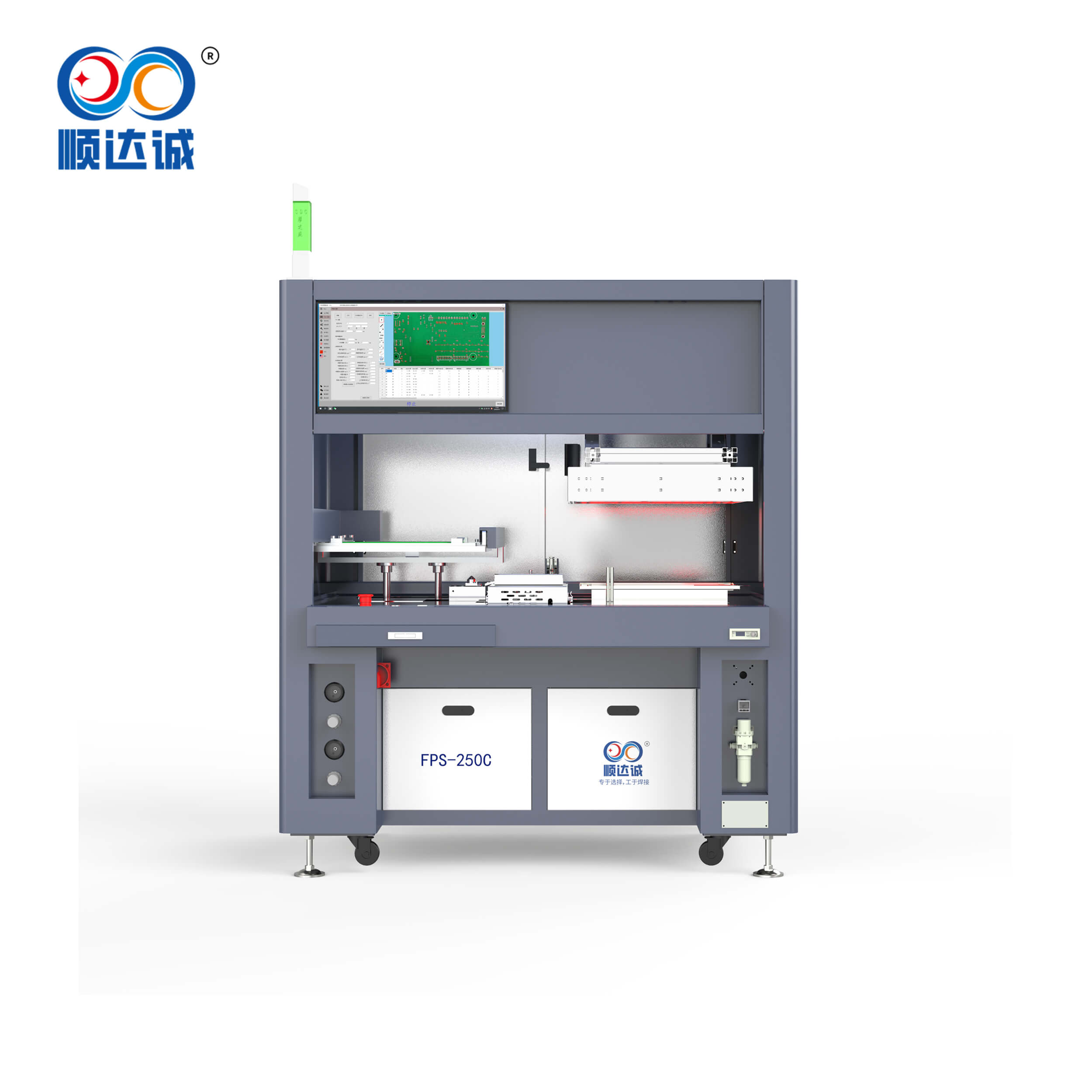
Evaluating Equipment: Sourcing an Industrial PCB Selective Soldering Machine
The Requirement for Dual Preheat Soldering Equipment
Heavy copper demands sustained thermal energy. You must evaluate machines with independent, closed-loop top and bottom preheaters. Single-heater systems fail to maintain the required delta-T. They allow thick copper planes to cool during the actual soldering phase. The board loses critical heat before the nozzle finishes its programmed path. Investing in reliable dual preheat soldering equipment solves this problem. It locks the core temperature in the optimal zone from start to finish.
Closed-loop systems use pyrometers to monitor the actual board temperature in real-time. They adjust heater output dynamically to prevent overheating or underheating. If the board gets too hot, the heaters back off. If it cools, they ramp up. This guarantees a stable thermal environment regardless of the ambient factory temperature or the specific board mass.
Nitrogen Inertion and Solder Wave Stability
High-purity nitrogen prevents dross formation at elevated solder pot temperatures. Operating above 300°C accelerates oxidation rapidly in ambient air. Nitrogen inertion blankets the wave, keeping the solder pure and fluid. You must maintain oxygen levels below 50 PPM for optimal results. Evaluate nozzle design for sustained wave stability. Pumping high volumes of solder into heavy thermal loads causes turbulence.
A well-designed industrial PCB selective soldering machine maintains a smooth, consistent wave. This ensures unbroken contact between the molten solder and the through-hole barrel. Wetted nozzles made from titanium or cast iron resist degradation. They provide a stable flow even at maximum pump RPM. A turbulent wave introduces air pockets into the joint, causing voids and weak connections.
Programmability for Variable Thermal Zones
Mixed-technology boards require variable thermal profiles. Assess software capabilities for programming different parameters on the same board. You might program a 5-second dwell with a high pump RPM for a heavy power connector. The very next joint might be a standard header requiring a 1-second dwell with a low pump RPM. The machine must switch parameters instantly and accurately.
Precise, repeatable machine control ensures consistency across production batches. It eliminates the guesswork from complex board assemblies. Advanced software allows you to define specific drag speeds, dip angles, and peel-off speeds for each joint. This level of control is mandatory when dealing with the unpredictable thermal dynamics of heavy copper planes.
Achieving 100% Through Hole Solder Fill on Thick Copper PCBs
Defining Success Criteria (IPC Class 3 Compliance)
Reviewing IPC-A-610 requirements sets the baseline for quality. Standard vertical fill requirements typically sit at 75%. High-reliability power applications often target a full 100% fill. Achieving complete through hole solder fill on thick copper PCBs guarantees maximum current carrying capacity. It also provides the mechanical strength needed for harsh environments.
Anything less risks field failures under heavy electrical loads. Automotive EV inverters and aerospace power supplies strictly enforce these Class 3 standards. You cannot fake a 100% fill. The process must be perfectly dialed in, combining optimal preheat, aggressive solder temperatures, and precise nozzle control.
Inspection and Verification Methods
Automated Optical Inspection (AOI) has severe limitations here. It cannot verify internal barrel fill or detect hidden voids. It only sees the top and bottom fillets. You must utilize 2D or 3D X-ray inspection. This reveals the exact volume of solder inside the barrel. Destructive cross-sectioning remains the ultimate validation tool. Cut the board open during the New Product Introduction (NPI) phase. Inspect the intermetallic bond and measure the exact fill percentage.
Run a sample batch of boards using the baseline thermal profile.
Perform 3D X-ray inspection on all heavy copper power nets to check for internal voiding.
Select the worst-performing board and perform destructive cross-sectioning on the power terminals.
Measure the intermetallic layer thickness to ensure proper metallurgical bonding.
Adjust preheat temperatures and nozzle dwell times based on the cross-section data.
Repeat the process until you achieve consistent 100% barrel fill across all sample boards.
Design for Manufacturability (DFM) Modifications
Thermal Reliefs and Pad Design
Process optimization cannot overcome poor board design. Standard thermal relief spoke dimensions are insufficient for heavy copper. The massive planes will still drain heat too quickly. You must calculate spoke width carefully. Balance the electrical current carrying capacity with thermal isolation during soldering. Wider spokes carry more current but increase thermal dissipation.
Narrower spokes solder easily but may act as fuses under heavy electrical load. Finding the exact middle ground dictates your production yield. Work closely with layout engineers to customize spoke geometry for each specific power net. Sometimes a 4-spoke design is necessary; other times a 2-spoke design provides better thermal isolation while still meeting the current requirements.
Component Spacing and Keep-Out Zones
Adjust clearance rules to accommodate larger, custom nozzles. High thermal transfer requires wider nozzle diameters. A standard 4mm nozzle will not transfer enough heat for a 6oz board. You might need an 8mm or 12mm nozzle. This means you need larger keep-out zones around through-hole components. You must protect adjacent SMD components from the extended radiant heat.
Prolonged selective soldering cycles generate significant local temperatures. Move sensitive capacitors or plastic connectors further away from the solder target. If a ceramic capacitor sits too close to the solder nozzle, it will crack from thermal shock.
Increase nozzle clearance by at least 3mm to 5mm around heavy power pins.
Relocate heat-sensitive SMDs, like plastic connectors or electrolytic capacitors, to the top side of the board.
Expand solder mask dams between closely spaced pads to prevent bridging during high-RPM wave flow.
Orient tall components to avoid blocking nitrogen flow from the nozzle.
Cost vs. Yield: Justifying Custom Selective Soldering Solutions
Wave Soldering vs. Manual Soldering vs. Selective Soldering
Operators struggle to achieve consistent fill manually on thick copper. Manual soldering leads to high defect rates and operator fatigue. It also causes thermal damage due to excessive iron dwell times as operators try to force the solder to flow. Wave soldering provides massive thermal energy but lacks precision. It requires expensive, custom-milled wave pallets to protect SMDs on mixed-technology boards.
Selective soldering adapts to different products with minimal mechanical changes. It significantly reduces setup time. This makes it easier to switch products in high-mix environments. It provides the thermal power of wave soldering with the precision of a robotic platform.
Soldering Method
Thermal Control Capability
Targeting Precision
Setup and Changeover Time
Manual Hand Soldering
Very Poor (Relies on operator skill)
Low (Prone to human error)
Minimal (No programming needed)
Traditional Wave Soldering
High (Global board heating)
Low (Requires physical masking)
High (Requires custom pallets)
Automated Selective Soldering
High (Targeted, programmable heating)
High (Pin-point accuracy)
Low (Software program based)
ROI on Custom Tooling and Nozzles
Evaluate the upfront cost of custom wetted nozzles and specialized fluxers. Compare this against the massive reduction in manual rework and scrap rates. Heavy copper boards are expensive to manufacture. Scrapping a single fully populated EV inverter board destroys profit margins for the day. Investing in custom selective soldering solutions pays for itself rapidly.
It improves overall reliability and guarantees IPC Class 3 compliance. Custom nozzles direct heat exactly where it is needed. They match the specific geometry of massive busbars or odd-form power terminals. They prevent thermal damage to the surrounding substrate. This targeted approach maximizes yield and eliminates costly downstream field failures.
Conclusion
Successfully soldering thick copper PCBs requires abandoning standard FR4 process parameters. It demands a holistic approach pairing DFM thermal reliefs with aggressive, sustained thermal management. Precise, programmable equipment is absolutely essential. When evaluating contract manufacturers or equipment, prioritize those demonstrating proven capability with dual preheat systems. Look for expertise in high-temperature flux management and closed-loop thermal profiling. Take the following actionable steps to improve your process today:
Initiate a DFM review focused specifically on thermal reliefs and keep-out zones for heavy copper nets.
Execute a thermal profiling trial using a dummy board with representative copper weights and layer counts.
Upgrade your flux chemistry to a high-solids, high-temperature formulation designed for extended preheat cycles.
Audit your current equipment for closed-loop, dual preheat capabilities.
FAQ
Q: What is the biggest challenge in thick copper PCB soldering?
A: The primary challenge is rapid heat dissipation. Thick copper planes and heavy component pins act as massive heat sinks. They pull heat away from the through-hole instantly. This causes the solder to freeze before achieving complete capillary fill, resulting in cold joints, incomplete barrel fill, and weak electrical connections.
Q: Why is dual preheat soldering equipment necessary for heavy copper?
A: Heavy copper requires the entire board core to reach 130°C to 150°C to allow solder to flow properly. Dual preheaters ensure uniform heating from both the top and bottom. This prevents the board from cooling down during the selective soldering process, maintaining the required thermal delta.
Q: Can wave soldering be used instead of selective soldering for thick copper?
A: Yes, but wave soldering mixed-technology boards requires expensive, custom-milled pallets to shield surface-mount components. Selective soldering offers superior precision. It directs heat and solder only to programmed areas, eliminating the need for pallets and requiring minimal mechanical changes between different product runs.
Q: Why is manual hand soldering not recommended for high thermal mass PCB soldering?
A: Manual soldering lacks the sustained, controlled thermal output required to heat heavy copper planes. Operators often leave the iron on the pad too long to force solder flow. This leads to inconsistent hole fill, cold solder joints, lifted pads, and severe thermal damage to the FR4 substrate.
Q: How do you achieve 100% through hole solder fill on thick copper PCBs?
A: Achieving complete fill requires a combination of optimized DFM thermal reliefs, high-activity and high-temperature flux, elevated core preheat temperatures, and extended solder nozzle dwell times. Multi-pass soldering techniques are also highly effective at overcoming the massive thermal mass without causing thermal shock.
Q: What DFM changes are required for a selective soldering thick copper PCB process?
A: Designers must implement larger thermal reliefs on power and ground plane connections. They must also increase keep-out zones around through-hole components to accommodate larger solder nozzles, and ensure adequate spacing to prevent radiant thermal damage to adjacent surface-mount components.
Q: What makes an industrial PCB selective soldering machine suitable for high thermal mass boards?
A: Key features include closed-loop dual preheating, highly stable nitrogen-inerted solder waves, and programmable dwell times per joint. The machine must also maintain high solder pot temperatures without excessive dross generation and utilize wetted nozzles capable of high thermal transfer.


