

- HomeProducts
-
What Causes PCB Warpage During Selective Soldering?
Views: 0 Author: Site Editor Publish Time: 2026-10-29 Origin: Site


Substrate deformation on the assembly line directly drives up scrap rates. It forces costly rework and compromises long-term field reliability. As electronics manufacturing shifts toward high-mix, high-density assemblies, engineers rely heavily on selective soldering. This process introduces severe localized thermal gradients. If thermal management fails, extreme temperature differentials induce irreversible substrate deformation. This fractures delicate intermetallic bonds before the board even leaves the machine.
Transitioning from reactive troubleshooting to proactive process engineering stabilizes yields. Resolving PCB warpage during soldering requires strict design-for-manufacturing rules. You must understand residual fabrication stresses and deploy advanced thermal management hardware. By controlling the thermal delta across the entire assembly, production teams eliminate the physical stresses that tear solder joints apart.
Key Takeaways
Localized Heat is the Primary Catalyst: Unlike reflow or wave soldering, selective soldering applies intense, localized heat, making precise thermal profiling critical to preventing substrate deformation.
Material and Design Vulnerabilities: Asymmetrical copper distribution, Coefficient of Thermal Expansion (CTE) mismatches, and the release of internal fabrication stresses are the structural prerequisites for warpage.
Advanced Preheating is Non-Negotiable: Relying solely on localized nozzle heat guarantees thermal shock; full-board preheating is required to stabilize the substrate.
Equipment Selection Drives Yield: Investing in a dual preheating selective soldering machine significantly reduces the thermal delta across the board, directly correlating to lower defect rates and higher placement accuracy.
The Physics of PCB Warpage in Selective Soldering
Understanding substrate deformation requires looking at the baseline physics of thermal dynamics. When a circuit board enters a soldering system, it undergoes rapid physical changes. The way the material absorbs, distributes, and reacts to thermal energy dictates whether the board remains flat or bows under pressure.
Localized Thermal Gradients vs. Global Heating
Wave soldering exposes the entire bottom surface of a circuit board to a uniform wave of molten solder. The global heat application allows the substrate to expand at a relatively consistent rate across its entire geometry. Selective soldering operates differently. It utilizes a miniature fountain of solder to target specific through-hole pins, leaving the rest of the board relatively cool.
This point-to-point heat application creates a massive temperature differential between the active soldering site and the surrounding FR4 material. The localized area expands rapidly while the cooler surrounding material resists that expansion. This mechanical conflict forces the substrate to bend. The steeper the thermal gradient, the more violent the resulting deformation. When a 280°C solder nozzle hits a board resting at 80°C, the localized expansion forces the rigid, cooler sections to act as a fulcrum, bowing the board upward or downward depending on the layer stackup.
CTE Mismatch in Multilayer PCB Selective Soldering
Circuit boards are composite structures. They consist of woven fiberglass, cured epoxy resin, copper foil, and solder mask. Each of these materials possesses a distinct Coefficient of Thermal Expansion (CTE). Copper expands at a different rate than the FR4 dielectric material.
During multilayer PCB selective soldering, the rapid heating and cooling phases force these materials to fight against one another. The copper traces want to elongate, but the fiberglass substrate restricts them. This differing expansion rate generates immense internal mechanical stress. When the stress exceeds the structural rigidity of the board, the entire assembly twists or bows to relieve the tension. High-layer-count boards with heavy 2oz or 3oz copper planes exacerbate this issue, as the sheer mass of the expanding copper easily overpowers the thin dielectric layers separating them.
PCB Thermal Stress During Soldering and the Glass Transition Temperature (Tg)
Every FR4 substrate has a Glass Transition Temperature (Tg). Below this threshold, the material remains rigid and glass-like. As the board approaches or exceeds its Tg, the epoxy resin softens, transitioning into a plasticized, rubbery state. In this state, the board loses its mechanical strength and becomes highly susceptible to bending.
Managing PCB thermal stress during soldering requires keeping the board properly supported while it is plasticized. If the board cools unevenly, or if tooling clamps lock it into a warped position while it drops back below its Tg, those mechanical stresses become permanently locked in. The board will retain its warped shape even after it returns to room temperature. Engineers must carefully match the preheat profile to the specific Tg rating of the board, whether it is standard Tg130 or high-temp Tg170 material.
The Release of Residual Fabrication Stresses
Substrate deformation on the assembly floor often originates at the bare board fabrication facility. PCB manufacturing involves high-pressure lamination presses and high-temperature curing cycles. These processes inherently trap mechanical stresses inside the core and prepreg layers.
When the bare board arrives at the assembly facility, it may appear perfectly flat. However, the moment the selective soldering nozzle applies liquidus temperatures to the substrate, those trapped internal stresses release violently. The sudden relaxation of the epoxy resin allows the board to snap into a deformed shape, severely compounding any warpage caused by the immediate thermal gradient. Baking boards prior to assembly can sometimes relieve these stresses, but it adds significant cycle time and handling costs to the production floor.
Downstream Impacts of Warpage on Assembly Yield
Substrate deformation directly degrades financial and operational metrics. Evaluating the true cost of warped boards requires auditing the specific defects they generate downstream. Upgrading equipment and auditing processes becomes easy to justify when you quantify the scrap rates tied to thermal deformation.
Solder Joint Defects, Bridging, and Short Soldering
Selective soldering relies on exact Z-axis positioning. The solder nozzle must maintain a precise standoff distance from the bottom of the board to ensure proper capillary action up the through-hole barrel. A warped board fundamentally alters this critical Z-axis height.
If the board bows upward, away from the nozzle, the solder wave fails to make adequate contact with the pins. This results in insufficient solder fill or complete short soldering. Conversely, if the board bows downward, toward the nozzle, the pins plunge too deeply into the solder pot. This displaces excess solder, causing bridging between adjacent pins and generating rogue solder balls across the substrate. Operators often waste hours chasing these defects, adjusting pump RPMs when the actual root cause is substrate deformation.
Drop-Jet Fluxer Alignment and Wetting Failures
Modern selective soldering systems use high-precision drop-jet fluxers to apply micro-droplets of flux exactly onto the target pads. These fluxers are calibrated for a specific focal distance. Substrate deformation alters the distance between the board and the fluxer head.
When the board warps, the flux droplets miss their target pads, landing on the solder mask instead. Without flux to strip away surface oxides, the molten solder cannot form a proper intermetallic bond. This lack of flux mimics severe surface contamination, leading to poor solder wetting, cold joints, and eventual field failures. You will often see operators manually brushing flux onto boards to compensate, which defeats the purpose of an automated process and introduces massive variability.
Component Shift, Alignment Issues, and BGA Open Circuits
Warpage does not just affect the through-hole components currently being soldered; it wreaks havoc on previously reflowed surface mount devices. When the board twists, it exerts sheer force on the existing solder joints. This leads to component placement accuracy degradation and severe alignment issues.
The compounding effect is most destructive on large Ball Grid Array (BGA) packages. BGAs often experience their own component-level warpage during thermal cycling. When a warping BGA interacts with a warping motherboard, the opposing forces fracture the brittle intermetallic layers. This dynamic routinely causes latent open circuits and cracks delicate Multi-Layer Ceramic Capacitors (MLCCs). These micro-cracks are notoriously difficult to detect during standard in-circuit testing and often only fail once the product reaches the end user.
Chassis Integration and Depaneling Failures
Even if a warped board passes electrical testing, it often fails mechanical assembly. Modern electronics feature tight-tolerance enclosures. A board with a pronounced bow will fail to slide into chassis guide rails or cause assembly interference with external connectors.
Furthermore, warped boards behave unpredictably during depaneling. When operators attempt to separate a deformed panel using a V-score cutter or a routing machine, the uneven stress distribution causes the FR4 to snap unpredictably. This splintering damages trace routing near the board edge and turns a fully assembled product into immediate scrap. The mechanical strain of forcing a warped board flat to fit into a housing also places permanent tension on every solder joint on the assembly.
Root Causes: Why Boards Warp During the Selective Process
Thermal deformation is rarely a random occurrence. It stems from specific process failures and design flaws that trigger mechanical instability. Breaking down these evaluation dimensions helps engineering teams isolate and eliminate the root causes.
Inadequate Preheating Strategies
The most common process failure is failing to bring the entire PCB assembly to a stable baseline temperature before the solder nozzle engages. If the board is cold when the 300°C solder wave hits it, thermal shock is guaranteed. PCB warpage in selective soldering spikes dramatically when facilities rely on single-zone or bottom-only preheaters for thick, high-mass boards.
Bottom-only preheating heats the underside of the board while the top side remains cool. This intentional temperature imbalance forces the board to bow immediately. High-mass boards require deep thermal soaking to mitigate internal stress release, which single-zone heaters simply cannot provide. A board with heavy ground planes acts as a massive heatsink, pulling energy away from the solder joint. If the preheat is inadequate, the machine must dwell longer on each joint, pumping even more localized heat into the substrate and worsening the warpage.
Poor Pallet and Fixture Design
Wave and selective soldering pallets are designed to support the board, but poorly designed fixtures actually cause warpage. The FR4 material must expand when heated. If the pallet restricts this natural thermal expansion, the board has nowhere to go but up or down.
Improper routing in the pallet, a lack of center support for wide boards, or excessively tight board clamps act as a straightjacket. When operators overtighten the clamps, the board buckles the moment it enters the preheat zone. Properly designed pallets allow for lateral expansion while providing rigid Z-axis support. Engineers must specify pallets made from high-grade composite materials that maintain their own dimensional stability at elevated temperatures. If the pallet warps, the board warps with it.
Asymmetrical Copper Distribution
Many warpage issues begin in the CAD software. Asymmetrical copper distribution creates a severe bimetallic strip effect during thermal cycling. If a designer places heavy, solid copper ground planes on the bottom layers of the board but leaves the top layers sparsely routed, the board will heat and expand unevenly.
The heavy copper side absorbs heat rapidly and expands aggressively. The sparse side absorbs heat slowly and resists expansion. This physical imbalance forces the board to curl. While assembly engineers cannot change the board design on the floor, they must identify asymmetrical copper to adjust their thermal profiles accordingly. Communicating these DFM violations back to the layout team is the only long-term fix for asymmetrical warpage.
Evaluating Precision Soldering Equipment for PCB Assembly to Prevent Warpage
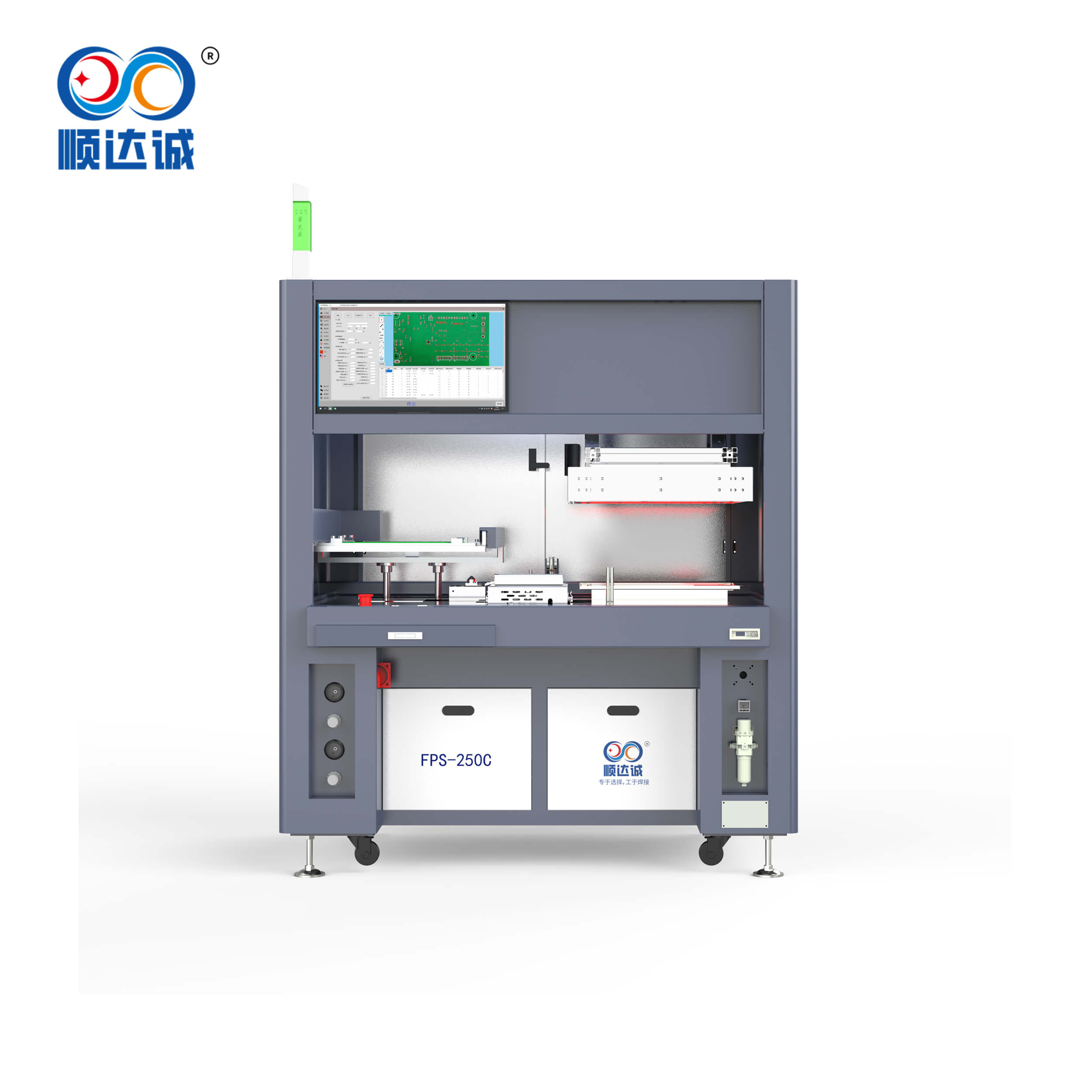
Solving thermal deformation requires hardware capable of manipulating heat with exact precision. When evaluating precision soldering equipment for PCB assembly, engineering teams must shortlist machines based entirely on their thermal management capabilities.
The Role of a Dual Preheating Selective Soldering Machine
High-mass assemblies demand dual preheating. This involves utilizing multiple preheat zones or top-and-bottom heating configurations to saturate the board with thermal energy evenly. A dual preheating selective soldering machine steps the temperature up gradually.
Gradual temperature stepping prevents thermal shock. It allows the internal stresses of the FR4 and copper layers to equalize before the liquid solder makes contact. By minimizing the temperature delta between the soldering point and the rest of the board, dual preheating maintains component alignment and keeps the substrate perfectly flat. Machines equipped with modular preheat zones allow engineers to build custom thermal profiles that soak the board at 100°C before ramping up to 140°C just prior to soldering.
Top Hot Air Bottom Infrared Preheating
Different thermal transfer methods yield different results. Bottom Infrared (IR) heating provides rapid energy transfer and deep penetration, making it excellent for driving heat into heavy copper planes. However, IR heating can be uneven depending on the color and reflectivity of the components and solder mask.
Top hot air provides uniform, convection-based stability. It wraps the top-side components in a blanket of consistent heat, regardless of their color or geometry. Combining these technologies into a top hot air bottom infrared preheating system is the industry standard. It allows engineers to process complex, heavy-copper multilayer boards rapidly without inducing the thermal imbalances that cause warpage.
Comparison of Preheating Technologies for Selective Soldering
Preheating Method
Heat Transfer Mechanism
Warpage Prevention Capability
Best Application
Bottom IR Only
Radiant energy targeting the underside of the PCB.
Low. Creates a high top-to-bottom temperature delta, often inducing bowing.
Thin, low-mass, single-sided consumer electronics boards.
Top Hot Air Only
Convection heating targeting the component side.
Moderate. Good uniformity but struggles to penetrate thick copper planes.
Medium-mass boards with sensitive top-side components.
Top Hot Air + Bottom IR
Combined radiant penetration and uniform convection.
High. Equalizes thermal stress across all layers simultaneously.
Thick, high-density, heavy-copper multilayer assemblies.
Closed-Loop Thermal Profiling and Z-Axis Compensation
Hardware is only as good as its control system. Relying on emitter temperature settings is dangerous because it does not reflect the actual temperature of the circuit board. Advanced machines utilize closed-loop pyrometers to monitor the actual board temperature in real-time, adjusting the heaters dynamically to maintain the exact profile.
Elite systems feature laser-based warp compensation. Even with perfect preheating, some boards will exhibit minor sagging due to their sheer weight. Laser sensors map the board's topography in real-time. The machine then dynamically adjusts the Z-axis height of the solder pot and fluxer to match the warped contour, completely preventing short soldering and bridging. This active compensation ensures the nozzle maintains a perfect 1.5mm standoff distance regardless of how the board behaves under heat.
Implementation Risks and Mitigation Strategies
Deploying advanced thermal controls introduces operational trade-offs. Production managers must balance the physics of soldering against the realities of factory throughput and maintenance schedules.
Balancing Cycle Time with Thermal Soak Requirements
The primary trade-off in warpage prevention is cycle time. Longer, more gradual preheat cycles drastically reduce warpage, but they inherently increase takt time. If a board requires a 90-second thermal soak, the machine cannot output a board every 60 seconds.
To mitigate this bottleneck, facilities should evaluate machines equipped with modular preheat stations or parallel processing capabilities. By staging multiple boards in a preheat tunnel simultaneously, the machine maintains high throughput while ensuring each individual board receives the adequate thermal soak required to remain flat. You can process board A in the solder module while board B and board C are soaking in the preheat zones.
Tooling and Carrier Maintenance
Solder pallets degrade over time. Titanium and composite carriers endure thousands of thermal cycles, flux exposure, and mechanical handling. Over time, the pallet itself can warp, transferring that mechanical deformation directly to the PCB it carries.
Implement a strict maintenance schedule for all carriers. Pallets must be checked for flatness using a surface plate. Operators must clean surface contamination daily to prevent hardened flux from creating uneven resting surfaces. Ensure all clamps actuate freely; seized clamps will lock the board in place, inducing severe mechanical stress during the heating cycle. Replace any pallet that shows signs of delamination or structural fatigue immediately.
Operator Training for Thermal Profiling
The greatest risk to thermal stability is human intervention. Operators under pressure to hit production quotas often bypass preheat zones or crank up IR emitters to speed up the process. This immediately triggers thermal shock and board warpage.
Mitigate this by implementing strict access controls on machine recipes. Lock out the ability to alter preheat times or temperatures without engineering approval. Conduct mandatory training on the use of thermocouple profiling boards. Operators must understand that validating thermal recipes with a physical profiler is the only way to guarantee the board is reaching activation temperature safely. Visual inspections are not a substitute for hard thermal data.
Conclusion
Substrate deformation during selective soldering is the destructive collision of asymmetrical board design, residual fabrication stresses, differing material physics, and inadequate thermal management. Relying on localized nozzle heat without preparing the substrate guarantees high defect rates, fractured BGA joints, and costly rework. To stabilize yields, engineering teams must prioritize precision soldering equipment offering top and bottom dual preheating combined with closed-loop thermal monitoring.
Take the following actions to eliminate substrate deformation in your facility:
Audit current scrap rates specifically for warpage-induced defects, isolating instances of BGA open circuits, short soldering, and chassis fitment failures.
Run comprehensive thermal profiles using thermocouple-equipped dummy boards on your heaviest, highest-density PCB assemblies to identify temperature deltas between the top and bottom layers.
Request equipment demonstrations from manufacturers, focusing strictly on their top hot air and bottom IR preheating capabilities.
Test laser-based Z-axis warp compensation features using your most problematic board designs during vendor evaluations.
Implement a weekly flatness and clamp-actuation inspection routine for all selective soldering pallets to ensure tooling is not inducing mechanical stress.
FAQ
Q: What is the acceptable IPC standard tolerance for PCB warpage?
A: The acceptable tolerance is defined by IPC-A-600 and IPC-A-610 standards. For circuit boards utilizing surface mount components, the maximum allowable bow and twist is 0.75%. For all other boards, such as those using only through-hole components, the maximum allowable bow and twist is 1.5%.
Q: How does selective soldering differ from wave soldering regarding thermal stress?
A: Wave soldering exposes the entire bottom surface of the board to molten solder, heating the substrate uniformly. Selective soldering applies intense, localized heat only to specific pins. This point-to-point heating creates severe localized thermal gradients, causing uneven expansion and higher thermal stress.
Q: Can component-level warpage worsen PCB warpage effects?
A: Yes. Large components, particularly BGAs, warp independently of the PCB during thermal cycles. When component warpage interacts with substrate warpage, the opposing mechanical forces create severe coplanarity issues. This dynamic frequently fractures brittle intermetallic layers, leading to latent open circuits.
Q: Can PCB warpage be reversed after soldering?
A: No. While some facilities attempt mechanical straightening or thermal baking to flatten a warped board, it is highly risky. These methods routinely fracture internal vias, tear copper traces, and break existing solder joints. It is not a viable or reliable production solution.
Q: Why do multilayer PCBs warp more easily during selective soldering?
A: Multilayer boards consist of varying materials, including copper planes, prepreg, and FR4 cores. Each material has a different Coefficient of Thermal Expansion (CTE). Rapid, localized temperature changes force these materials to expand at different rates, compounding internal stresses and forcing the board to bend.
Q: How does top hot air and bottom IR preheating reduce warpage?
A: This combination ensures the entire mass of the board reaches the required activation temperature uniformly from both sides. Bottom IR penetrates heavy copper planes, while top hot air provides stable convection. This minimizes the thermal shock when the liquid solder nozzle engages the board.
Q: Does the design of the soldering pallet affect PCB warpage?
A: Absolutely. Poorly designed pallets that grip the board too tightly prevent natural thermal expansion. When the FR4 material heats up and tries to expand, restrictive clamps force the board to buckle upward or downward to relieve the mechanical tension.


