

- HomeProducts
-

Selective Soldering Nozzles: Types, Sizes, and Applications
Views: 0 Author: Site Editor Publish Time: 2026-11-05 Origin: Site


The transition toward high-density interconnects and mixed-technology boards has rendered traditional wave soldering impractical for many modern assemblies, necessitating highly controlled, localized soldering methods. Achieving repeatable, defect-free through-hole joints without causing thermal damage to adjacent surface-mount components requires exact control over solder volume, fluid dynamics, and thermal transfer. Selecting the correct selective soldering nozzle—balancing material composition, diameter, and wetting characteristics—is the primary variable in optimizing cycle times, minimizing rework, and ensuring IPC-compliant hole fill. Modern assemblies demand customizable applications tailored to specific components, ensuring that molten solder is directed precisely where needed with minimal impact on the rest of the board. You must match the tooling to the board topography to maintain high production yields and process stability.
Nozzle material (wettable vs. non-wettable) dictates solder flow dynamics, wave stability, and maintenance schedules, particularly in aggressive lead-free environments.
Matching nozzle diameter to component pitch and thermal requirements is critical; standard sizes range from micro-nozzles for tight clearances to the versatile D8mm selective soldering nozzle for heavy copper planes.
High-mix, high-volume production environments benefit from a custom selective soldering machine configuration utilizing dual-functioning, multi-nozzle (mini-wave), or hybrid full-wave setups.
Rigorous evaluation of nozzle geometry prevents common defects such as bridging, solder balling, and insufficient hole fill in dense PCB assemblies.
Success Criteria for Selective Soldering Operations
Defining the Baseline
Achieving IPC-A-610 Class 3 hole fill requirements demands strict process control on the shop floor. Class 3 typically mandates 75% or greater vertical fill inside the plated through-hole. Operators must achieve this penetration without causing collateral thermal damage to adjacent surface-mount devices. The process window remains incredibly narrow. Excessive heat damages sensitive components or causes board delamination, while insufficient heat leads to cold joints, poor wetting, and incomplete capillary action. You have to deliver enough thermal energy to pull the solder up the barrel without exceeding the thermal limits of the surrounding FR4 material.
Problem Framing
Engineers face significant challenges when processing thick backplanes, high-mass components, and thermally sensitive devices on a single board assembly. Thick multi-layer boards act as massive heat sinks. They draw thermal energy away from the solder joint rapidly. High-mass components like power relays, transformers, or industrial connectors require prolonged heat exposure to reach liquidus temperatures. Conversely, adjacent micro-controllers or plastic housings melt or degrade under similar thermal loads. Balancing these conflicting requirements defines the core engineering challenge on the production line.
Heat Sinking: Heavy copper ground planes pull heat away from the through-hole barrel, causing solder to freeze prematurely.
Component Proximity: Dense layouts place delicate 0402 or 0201 packages within millimeters of massive through-hole pins.
Flux Outgassing: Tight barrel clearances trap flux volatiles, leading to voids inside the solder joint if the approach angle is incorrect.
Thermal Shock: Rapid localized heating warps the PCB if pre-heating profiles are not dialed in correctly.
The Nozzle's Role
The nozzle acts as the primary interface for thermal delivery and fluid dynamics. In precision through hole selective soldering, the nozzle geometry directly influences the time-above-liquidus (TAL). It controls exactly how the solder wave contacts the pin and pad. The flow rate, wave height, and surface tension at the nozzle tip determine how efficiently heat transfers into the barrel. A poorly matched nozzle results in frozen solder, bridging between adjacent pins, or thermal shock to the assembly.
Core Types of Selective Soldering Nozzles
Wettable Nozzles
Wettable nozzles rely on specialized alloys that allow molten solder to adhere to their outer surfaces. Solder flows continuously over the nozzle edge. This creates a stable, directional wave guided by surface tension. The liquid metal maintains a consistent dome shape, providing a predictable contact area for the PCB.
These nozzles offer superior thermal transfer. The continuous flow of fresh, hot solder directly contacts the joint, breaking through oxidation layers quickly. They are ideal for tight pitches, multi-directional drag soldering, and breaking solder bridges during the peel-off phase. The surface tension helps pull excess solder away from adjacent pins as the board moves away from the wave.
However, wettable nozzles require frequent maintenance. Operators must perform regular de-drossing and re-tinning to keep the surface active. The aggressive nature of lead-free alloys degrades the wetted surface over time. This results in a higher consumable cost and a shorter operational lifespan compared to alternative designs. If the nozzle loses its wetting capability, the wave becomes erratic and unpredictable.
Non-Wettable Nozzles
Non-wettable nozzles utilize materials that repel molten solder. Solder pumps up through a specialized, treated material without adhering to the exterior. Common materials include cast iron, titanium, or proprietary ceramic coatings. The solder simply crests at the top of the bore and falls back into the bath.
These designs require significantly lower maintenance. They reduce dross generation because less surface area is exposed to oxygen. They are highly durable against the leaching effects of high-tin, lead-free alloys like SAC305. Operators spend less time cleaning and replacing tooling, keeping the machine running longer between interventions.
The primary drawback is wave stability. Controlling the wave dynamics is more difficult during highly precise drag soldering. The lack of surface tension on the nozzle edge can cause the wave to fluctuate slightly in height. They are generally better suited for point-to-point dip soldering rather than complex routing paths across fine-pitch components.
Dual-Functioning and Specialized Nozzles
Manufacturers often deploy nozzles designed for specific geometries to overcome production bottlenecks. Jet waves use high-velocity solder streams to penetrate deep cavities or reach pins surrounded by tall components. Multi-wave plates allow simultaneous soldering of multiple component leads, acting like a miniature traditional wave soldering machine tailored to a specific board layout.
Dual-functioning nozzles and mini-wave setups provide customizable applications tailored to specific, high-mass components. They ensure minimal thermal impact on the rest of the board. An operator can program a wide nozzle for a massive power connector, then switch to a micro-nozzle for a delicate sensor on the same assembly using a dual-pot system.
Engineers must balance trade-offs on the floor. Single-point precision from a micro-nozzle offers ultimate flexibility but slows down cycle times significantly. Multi-point throughput from custom tooling plates speeds up production but requires expensive, dedicated fixtures for every single board design revision.
Feature
Wettable Nozzles
Non-Wettable Nozzles
Solder Flow Mechanism
Flows over the edge, guided by surface tension.
Pumps through the center, repelled by the exterior.
Thermal Transfer
Excellent; continuous fresh solder contact.
Moderate; dependent on pump pressure and wave height.
Best Application
Drag soldering, tight pitches, fine-pitch connectors.
Dip soldering, high-volume point-to-point joints.
Maintenance Level
High; requires daily re-tinning and de-drossing.
Low; highly resistant to alloy leaching.
Lifespan (Lead-Free)
Shorter; degrades under high-tin exposure.
Longer; titanium or coated iron resists corrosion.
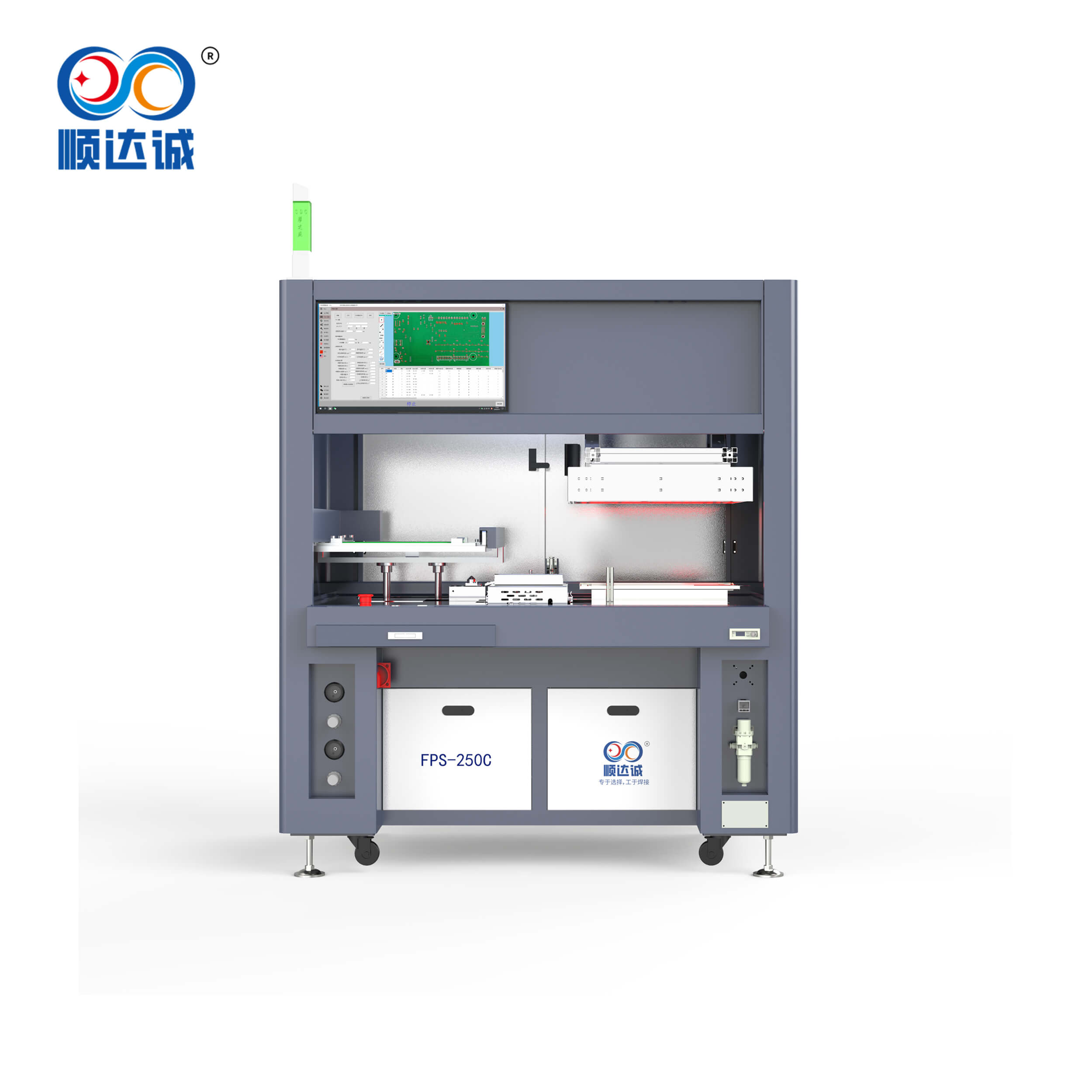
Evaluating Selective Soldering Nozzle Sizes and Geometries
Standard vs. Micro Nozzle Diameters
Engineers must align selective soldering nozzle sizes with the required keep-out zone (KOZ) and component pin pitch. The KOZ dictates the maximum allowable outer diameter of the nozzle. If the nozzle is too large, radiant heat or stray solder will reflow adjacent SMDs. If it is too small, it extends cycle times unnecessarily and fails to deliver enough heat.
Micro-nozzles (under 3mm in diameter) present specific limitations on the production floor. They risk freezing or poor hole fill on heavy copper layers. The small volume of flowing solder lacks sufficient thermal mass to overcome the heat dissipation of a thick ground plane. The solder cools before reaching the top of the barrel, resulting in incomplete capillary action and rejected boards. You should only use micro-nozzles when spatial constraints absolutely demand them.
The Role of the D8mm Selective Soldering Nozzle
The 8mm diameter serves as a reliable baseline for general through-hole components. Connectors, relays, and electrolytic capacitors generally process well with this size. The D8mm selective soldering nozzle provides a stable, manageable wave that fits between moderately spaced components without spilling over.
This size balances adequate thermal delivery with manageable spatial constraints. It carries enough molten solder to heat a standard multi-layer board quickly. Simultaneously, its footprint remains small enough to navigate moderately dense boards without requiring excessive keep-out zones. It represents the optimal middle ground for high-mix production where you want to minimize nozzle changeovers.
Selecting the Optional Solder Nozzle Diameter
Determining the optimal internal and external diameter requires a strict calculation framework. Engineers must evaluate the annular ring size, pin length, and adjacent component clearance. The internal diameter must encompass the entire pad to ensure proper wetting. The external diameter must clear the nearest SMD by at least 1.5mm to prevent collateral reflow.
Geometry impacts performance heavily. Nozzle length, wall thickness, and exit angle alter wave height and stability. Thicker walls retain heat better but increase the outer footprint. The exit angle determines how smoothly the solder peels away from the pin, which directly affects bridging. Proper geometry also maximizes nitrogen shielding efficiency, trapping the inert gas around the wave to prevent oxidation. Selecting the correct optional solder nozzle diameter prevents 90% of common soldering defects before the board even enters the machine.
Nozzle Diameter (Internal)
Typical Component Application
Minimum Keep-Out Zone (KOZ)
2mm - 3mm (Micro)
Single pins, tight sensors, dense mixed-tech.
1.5mm - 2.0mm
4mm - 6mm
Standard headers, small capacitors, LEDs.
2.5mm - 3.0mm
8mm (D8mm)
Relays, power connectors, electrolytic caps.
3.5mm - 4.0mm
10mm - 12mm+
Heavy ground planes, large industrial terminals.
5.0mm+
Application Matching: Selective Soldering for Dense PCB Assemblies
Precision Through Hole Selective Soldering Techniques
Optimizing approach angles and peel-off speeds is mandatory for multi-row connectors and fine-pitch components. A perpendicular approach often traps flux gases inside the barrel, causing voids. Approaching at a slight 7 to 10-degree angle allows outgassing. Slowing the peel-off speed at the end of a drag soldering run utilizes surface tension to pull excess solder away, preventing bridges between closely spaced pins.
Operators must choose between dip soldering and drag soldering based on the layout. Dip soldering lowers the board onto a multi-point nozzle plate. It is fast but requires dedicated tooling. Drag soldering uses a single-point nozzle to route across the board. Wettable nozzles with angled tips support drag soldering best, while flat, non-wettable nozzles excel in dip applications. Implementing selective soldering for dense PCB assemblies requires mastering both techniques and knowing when to apply them.
Managing Keep-Out Zones (KOZ)
Navigating densely populated boards requires advanced spatial strategies. Modern designs often place SMDs within 1-3mm of through-hole pins. The robotic gantry must position the nozzle with sub-millimeter accuracy. The wave height must remain absolutely consistent to avoid spilling over the pad boundaries and destroying adjacent micro-components.
Component-specific tailoring adapts the nozzle approach for unique geometries. The system must isolate thermal energy from adjacent delicate sensors or micro-BGAs. Engineers program custom routing paths that approach from the side with the most clearance. They adjust pump RPM dynamically to lower the wave height when passing near sensitive areas, then increase it when hitting a heavy ground pin.
Tooling solutions provide physical barriers against heat and solder. Custom nozzle shrouds direct nitrogen flow precisely, cooling adjacent areas while inerting the joint. Localized nitrogen inerting prevents oxidation and improves wetting speeds. Precise programmable robotic arms execute these complex movements flawlessly, preventing collateral reflow and ensuring repeatable quality across thousands of boards.
Custom Selective Soldering Machine Configuration and Scalability
Single vs. Multi-Nozzle (Mini-Wave) Systems
Scaling production requires evaluating machine architecture. Single-nozzle systems offer high flexibility but lower throughput. Configuring machines with up to six individual mini-waves allows simultaneous processing of high-volume assemblies. Multiple pots operate independently, applying solder to different regions of the board concurrently, drastically reducing cycle times.
Hybrid system integration combines selective mini-wave modules with traditional full-wave capabilities. A single custom selective soldering machine configuration might feature an 18-inch wave module for bulk processing, followed by selective modules for sensitive components. This handles mixed-technology boards with maximum throughput, eliminating the need for separate wave and selective routing lines on the factory floor.
Robotic integration leverages programmable arms for dynamic nozzle positioning. Multi-axis robots adjust the tilt, yaw, and insertion angle of the board over the stationary nozzle. They enable varied wave heights and on-the-fly parameter adjustments. This flexibility accommodates complex board topographies that fixed-gantry systems simply cannot process without causing defects.
Flux Applicator and Pre-Heating Integration
Nozzle selection must strictly align with drop-jet fluxer precision. If the nozzle diameter is 6mm, the fluxer must deposit a spot no larger than 7mm. Overspraying flux leaves corrosive residues on the board that fail ionic contamination testing. Underspraying prevents proper wetting. The thermal capacity of IR or convection pre-heaters must also match the nozzle's heat delivery. The board must reach the proper top-side temperature (typically 100°C to 120°C) before the solder wave makes contact.
System-level trade-offs require evaluating capital expenditure against required throughput. Multi-nozzle systems and hybrid configurations cost significantly more upfront. They also increase programming complexity for the engineering team. However, the cycle time reductions often justify the investment in high-volume automotive, aerospace, or telecommunications manufacturing environments.
Implementation Risks and Maintenance Realities
Lead-Free Alloy Challenges
Lead-free alloys, particularly SAC305 and SN100C, present severe material degradation challenges. High tin content acts as a solvent, dissolving the iron and steel used in standard nozzles. This aggressive, corrosive nature compromises nozzle integrity rapidly. The inner bore widens, altering fluid dynamics and wave stability, which leads to inconsistent hole fill.
Mitigation requires selecting hardened nozzle materials. Titanium and specialized ceramic coatings resist tin leaching effectively. Optimizing nitrogen flow via specialized shrouds reduces dross formation. Dross acts as an abrasive, accelerating wear on the nozzle tip. Controlling pump RPM limits mechanical wear on the impeller and the nozzle walls, extending the maintenance interval and saving money on consumables.
Defect Troubleshooting and Maintenance Schedules
Identifying the root causes of common failures prevents extended downtime. Clogged nozzles usually stem from inadequate fluxing or excessive dross pulled into the pump. Degraded wetting on wettable nozzles indicates oxidation or alloy depletion. Inconsistent pump pressure often points to dross buildup in the impeller housing. Solder webbing suggests insufficient pre-heating or exhausted flux.
Establishing a strict maintenance schedule is non-negotiable for process stability.
Daily: De-dross the solder pot and re-tin wettable nozzles using a dedicated flux and solid solder wire.
Weekly: Verify wave height calibration with a glass gauge to ensure the solder contacts the board precisely.
Monthly: Perform ultrasonic cleaning in an adipic acid solution to remove baked-on flux residues from the nozzle assembly.
Quarterly: Inspect the impeller and pump housing for wear and tear, replacing parts before they cause pressure drops.
Conclusion
The selective soldering nozzle is not a generic consumable. It represents the most critical tooling decision in the selective soldering process. The nozzle directly dictates thermal transfer efficiency, routing flexibility, and overall defect rates. A misapplied nozzle guarantees bridging, poor hole fill, and thermal damage to adjacent components.
Base your initial nozzle selection on the most restrictive keep-out zone on your standard PCB assemblies. Identify the tightest clearance, select a nozzle that fits safely, and then scale up in diameter wherever clearances allow. Maximizing thermal mass is always preferable when space permits to ensure robust hole fill.
Audit your current PCB designs to map out the tightest keep-out zones and component pitches.
Standardize on an 8mm diameter nozzle for baseline thermal profiling on moderately dense boards.
Conduct a thermal profiling test utilizing both a standard nozzle and a micro-nozzle to establish baseline capabilities.
Implement a strict daily maintenance schedule for ultrasonic cleaning and re-tinning of wettable nozzles.
Test micro-nozzles on scrap heavy-copper boards to verify adequate vertical hole fill before finalizing production parameters.
FAQ
Q: What is the difference between wettable and non-wettable selective soldering nozzles?
A: Wettable nozzles allow molten solder to adhere to their outer surface, creating a highly stable, directional wave ideal for drag soldering and tight pitches. Non-wettable nozzles repel solder, pumping it through a treated core. They require significantly less maintenance and resist lead-free corrosion but are generally better suited for dip soldering.
Q: How do I determine the correct selective soldering nozzle sizes for my PCB?
A: Measure the keep-out zone (KOZ) around the target through-hole pins. The nozzle's outer diameter must clear adjacent surface-mount components by at least 1.5mm to prevent thermal damage. Choose the largest diameter that fits within this clearance to maximize thermal mass and ensure proper hole fill.
Q: When is it best to use a D8mm selective soldering nozzle?
A: The 8mm nozzle is the industry standard for general through-hole components like relays, connectors, and electrolytic capacitors. It provides an optimal balance between adequate thermal delivery for multi-layer boards and a compact footprint for navigating moderately dense assemblies.
Q: How does nitrogen inerting affect selective soldering nozzle performance?
A: Nitrogen inerting displaces oxygen around the solder wave, preventing the formation of dross (oxide). This drastically reduces maintenance, improves the wetting speed of the solder, and prevents bridging. It also extends the lifespan of wettable nozzles by protecting the tinned surface from rapid oxidation.
Q: What is the minimum keep-out zone (KOZ) required for precision through hole selective soldering?
A: A standard minimum KOZ is typically 1.5mm to 3mm from the edge of the through-hole pad to the nearest surface-mount component. This distance accommodates the nozzle wall thickness, the solder wave spillover, and the radiant heat zone, preventing collateral reflow of adjacent devices.
Q: How do lead-free alloys impact the lifespan of selective soldering nozzles?
A: Lead-free alloys, such as SAC305, have a high tin content that aggressively dissolves standard metals. This corrosive action leaches iron from the nozzle, widening the bore and degrading the wetted surface. Hardened materials like titanium or ceramic coatings are required to withstand this degradation.
Q: How often should wettable selective soldering nozzles be re-tinned or replaced?
A: Wettable nozzles typically require daily maintenance. Operators should de-dross and re-tin the nozzle at the start of every shift to maintain proper surface tension. Depending on production volume and alloy aggressiveness, the nozzle itself may need replacement every few weeks to a few months.


