

- HomeProducts
-

How Selective Wave Soldering Improves PCB Assembly Efficiency
Views: 0 Author: Site Editor Publish Time: 2026-08-21 Origin: Site


Modern printed circuit boards pack immense functionality into shrinking physical footprints. This drive for miniaturization creates highly complex, mixed-technology designs. Surface-mount technology components share tight board space with legacy through-hole connectors, relays, and capacitors. Traditional manufacturing methods struggle to handle this architectural complexity efficiently. Manual hand-soldering incurs massive labor expenses and yields inconsistent joint quality across production batches. Traditional wave soldering exposes the entire board to molten alloy, wasting raw materials and risking severe thermal damage to sensitive microchips. Furthermore, protecting delicate components during traditional wave processes requires custom masking and expensive machined pallets.
Implementing selective wave soldering emerges as a precision-driven electronics manufacturing solution to solve these exact bottlenecks. This technology bridges the gap between high-volume throughput demands and strict quality control requirements. It targets specific joints with pinpoint accuracy, leaving the rest of the board untouched. This targeted approach ultimately lowers the operational burden per board without compromising mechanical reliability. Manufacturers achieve superior barrel fill, eliminate masking steps, and accelerate their overall production timelines.
Precision over Volume: Selective wave soldering targets individual through-hole joints, eliminating the need for protective masking and protecting sensitive adjacent SMT components from thermal shock.
Defect Reduction & Joint Durability: Localized flux application and controlled mini-waves drastically reduce common defects like solder bridging and icicling, while ensuring superior barrel fill for highly durable, reliable joints.
Cost Efficiency & Agility: While the initial CapEx for a selective wave soldering machine is significant, the elimination of manual rework, masking materials, and custom pallets drives a strong long-term ROI, particularly in High-Mix, Low-Volume (HMLV) environments.
Ideal Use Case: Best suited for high-density, double-sided PCBs with mixed components where traditional wave soldering would cause unacceptable defect rates or thermal damage.
The Core Problem: Limitations of Traditional Soldering in Mixed-Technology PCB Assembly
Thermal Stress and Component Degradation
Thermal management dictates the success or failure of mixed-technology assembly. Sensitive surface-mount components must remain strictly below their critical temperature thresholds during processing. Exposing an entire FR4 circuit board to a traditional solder wave creates massive, uncontrolled thermal shock. The glass transition temperature of standard FR4 material limits how much heat the board can absorb before structural damage occurs. This sudden heat transfer risks catastrophic board delamination and internal layer separation.
Pad lifting frequently occurs under these harsh thermal conditions due to coefficient of thermal expansion mismatches between the copper pads and the fiberglass substrate. Component failure rates spike dramatically when delicate microprocessors face broad, sustained thermal exposure. Ceramic capacitors are especially vulnerable to micro-cracking when subjected to rapid temperature spikes. Precision targeted heating prevents this degradation entirely by isolating the thermal energy only to the pins that require metallurgical bonding.
The Hidden Costs of Masking and Custom Pallets
Mixed-technology boards introduce a severe operational bottleneck on the factory floor. Traditional wave soldering requires physical barriers to shield bottom-side SMT parts from the molten alloy. Operators must apply polyimide tape or liquid peelable solder masks entirely by hand. Alternatively, engineering teams must design and purchase custom-machined composite wave solder pallets. Applying, routing, and removing these protective barriers wastes countless labor hours every shift.
Consider the standard manual masking workflow that destroys production efficiency:
Operators review the assembly drawing to identify keep-out zones.
Workers manually cut and apply high-temperature polyimide tape over sensitive SMT components.
Technicians apply liquid peelable mask to specific vias and wait for it to cure.
The board runs through the traditional wave soldering machine.
Operators manually peel off the tape and cured liquid mask, risking damage to adjacent components.
Inspectors check the board for adhesive residue left behind by the tape.
This non-value-added preparation work creates massive workflow bottlenecks. It forces manufacturers to hire dedicated masking personnel, inflating labor overhead without adding any functional value to the final product.
Inconsistencies in Manual Through Hole Soldering
Many assembly facilities default to manual hand-soldering to process complex mixed boards. This alternative introduces significant quality control risks. Human error inevitably leads to inconsistent joint volumes and varying thermal profiles across production batches. Operators struggle to maintain precise temperature control and dwell times during long, fatiguing shifts. A technician might hold the iron on a heavy ground plane pin for five seconds, but only two seconds on the next board, resulting in a cold solder joint.
You cannot scale manual labor effectively to meet mid-to-high volume production schedules while maintaining IPC-A-610 Class 3 standards. Achieving 75% or 100% barrel fill on thick, multi-layer boards with heavy copper planes requires sustained, controlled heat that manual irons struggle to deliver consistently. Reliable through hole soldering requires repeatable, machine-driven precision that human hands simply cannot guarantee over thousands of consecutive joints.
Mechanics of Selective Wave Soldering: How the Technology Works
Localized Flux Application (Drop-Jet Technology)
Modern automated soldering equipment utilizes advanced drop-jet fluxers to achieve extreme chemical precision. The system fires micro-droplets of flux only onto the specific pins requiring metallurgical bonding. This highly targeted approach drastically reduces chemical waste and minimizes volatile organic compound emissions on the factory floor. Unlike spray fluxers that coat the entire bottom of the board, drop-jet valves operate much like an inkjet printer, depositing flux in exact coordinates.
This precision eliminates extensive post-assembly cleaning requirements. Boards emerge from the machine exceptionally clean, preventing long-term ionic contamination issues and dendritic growth in the field. When using no-clean flux formulations, the localized application ensures that any unactivated flux residue remains isolated to the immediate joint area, rather than spreading across sensitive high-impedance traces.
Precision Pre-Heating
Preventing thermal shock requires a highly controlled pre-heating phase. Systems deploy top and bottom infrared or forced convection heaters to elevate board temperatures gradually. These heaters activate the applied flux gently, preparing the surface chemistry for optimal wetting. They focus thermal energy specifically on the necessary thermal mass of the target joints. This localized heating strategy prepares the specific connection without baking the entire printed circuit board assembly unnecessarily.
Proper pre-heating also prevents the molten solder from freezing prematurely when it contacts a heavy copper ground plane. By raising the internal board temperature to the correct soak profile, the pre-heaters ensure that the capillary action can pull the molten alloy all the way up through the plated through-hole. Convection heaters provide excellent temperature uniformity, while quartz IR heaters offer rapid response times for quick profile adjustments.
The Mini-Wave Solder Nozzle
The core mechanism relies on a programmable, multi-axis robotic nozzle assembly. This titanium nozzle pumps a dynamic, localized mini-wave of molten solder directly to individual pins. An internal impeller creates a stable, dross-free solder dome. The robotic arm moves with pinpoint accuracy across the board topography. It solders each connection sequentially based on exact programmed coordinates, adjusting dwell times dynamically for different pin masses.
Wettable nozzles allow the solder to flow smoothly over the edge, creating a highly stable wave height. This stability is mandatory for achieving consistent contact with the through-hole pins without flooding adjacent surface-mount components. The system controls the pump speed precisely to maintain the wave height, even as the volume of solder in the pot fluctuates slightly during operation.
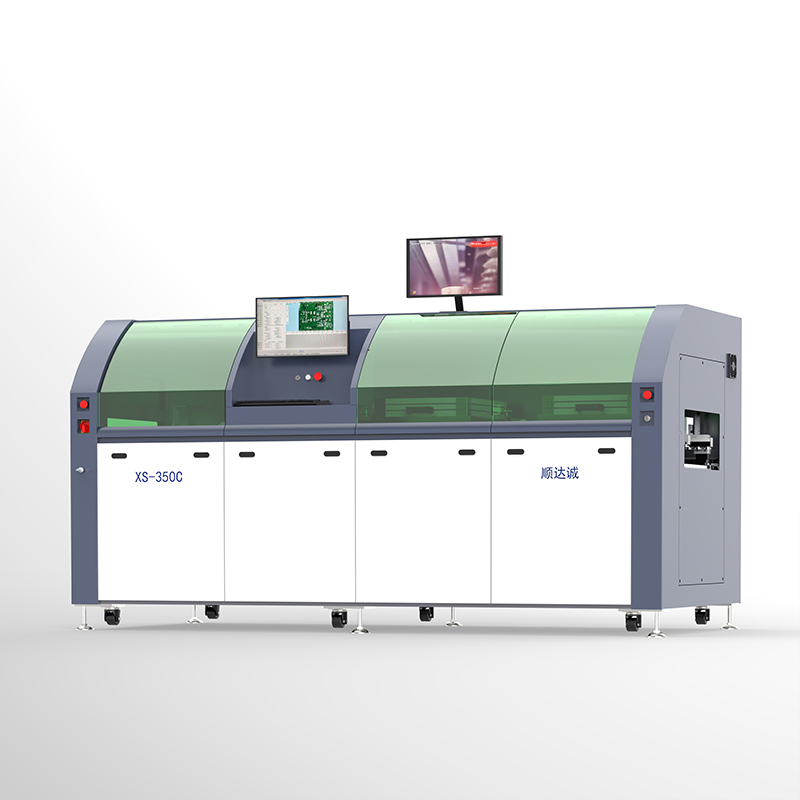
How a Selective Wave Soldering Machine Drives Assembly Efficiency
Eliminating Non-Value-Added Process Steps
A dedicated selective wave soldering machine streamlines the entire production floor layout. It removes manual masking and taping stations from the workflow completely. Operators no longer waste valuable time loading boards into heavy custom pallets and unloading them post-wave. Post-soldering wash cycles become largely obsolete due to the minimal, localized flux application.
Removing these cumbersome steps accelerates the overall prep-to-pack timeline significantly. A board that previously required twenty minutes of masking preparation now moves directly from the SMT reflow oven to the selective soldering cell. This continuous flow manufacturing model reduces work-in-progress inventory and increases daily factory output. Floor space previously dedicated to pallet storage and masking stations can be repurposed for revenue-generating assembly lines.
Drastic Reductions in Rework and Enhanced Joint Durability
Precise control over nozzle contact time dictates final joint quality. The operating system manages wave height, flow dynamics, and peel-off speed perfectly for every unique pin. This mechanical control utilizes capillary action to ensure consistent, complete barrel fill. It minimizes solder bridges and prevents sharp icicles from forming on lead tips. The peel-off speed—the rate at which the board separates from the solder wave—is programmed to draw excess solder back into the pot, leaving a perfect fillet.
These mechanically durable joints easily survive harsh field conditions, thermal cycling, and high-vibration environments. When soldering heavy connectors used in automotive or aerospace applications, the machine can be programmed to dwell longer on specific pins to ensure the heat penetrates the entire multi-layer board. This eliminates the need for technicians to touch up incomplete joints with a manual iron, drastically reducing rework rates.
Optimizing Material Consumption
Traditional wave pots hold massive amounts of molten alloy, often exceeding five hundred kilograms. Selective systems use a mere fraction of that volume, typically holding around fifteen kilograms. This drastic reduction in solder alloy usage saves substantial raw material resources. Smaller exposed solder surface areas mean significantly reduced dross formation. Less dross translates directly to lower material waste and greatly reduced maintenance overhead for the engineering team.
Process Parameter
Traditional Wave Soldering
Selective Wave Soldering
Solder Pot Capacity
400 - 600 kg
10 - 25 kg
Flux Consumption
High (Full board spray)
Very Low (Drop-jet targeted)
Dross Generation
High (Large exposed surface)
Minimal (Nitrogen shrouded mini-wave)
Masking Required
Yes (Tape, liquid, or pallets)
No
Agility in High-Mix, Low-Volume (HMLV) Production
Modern PCB assembly demands rapid adaptability to changing client orders. Software-driven changeovers allow manufacturers to switch between entirely different PCB designs instantly. Operators simply scan a barcode to load a new robotic program file. The machine automatically adjusts the fluxer coordinates, pre-heat profiles, and soldering paths without any physical tooling changes.
This digital approach provides unmatched manufacturing flexibility on the factory floor. It eliminates the long lead times and physical storage requirements associated with designing and machining dedicated composite tooling. In a high-mix environment where a facility might run ten different board designs in a single shift, this agility prevents hours of machine downtime. The equipment adapts to the product, rather than forcing the product to adapt to the equipment.
Selective Soldering vs. Traditional Wave Soldering: An Evaluation Framework
Overall Process Speed vs. Machine Throughput Trade-offs
Traditional wave soldering runs faster at the bare machine level. It excels at processing simple, high-volume, purely through-hole boards in seconds. A traditional wave can solder a thousand pins simultaneously as the board passes over the crest. However, selective soldering wins decisively when factoring in the total end-to-end cycle time. It eliminates prep work, masking application, pallet handling, and extensive manual rework.
For complex mixed-technology boards, the comprehensive process speed heavily favors the selective approach. While the robotic nozzle might take sixty seconds to solder fifty pins point-to-point, the elimination of thirty minutes of manual masking makes the selective process vastly superior in total takt time. Manufacturers must evaluate the entire value stream, not just the seconds spent inside the soldering machine.
Board Complexity and Component Density Thresholds
Engineering decision criteria often come down to physical clearance rules on the bare board. Examine the distance between through-hole pins and adjacent surface-mount components. When clearances drop below three millimeters, traditional wave processing becomes impossible without causing collateral damage. The molten wave will inevitably bridge the through-hole pin to the adjacent SMT pad, or reflow the SMT component entirely, washing it into the solder pot.
High component density mandates a targeted, robotic approach. Selective soldering becomes mandatory to navigate these tight board topographies safely without reflowing adjacent microchips. The mini-wave nozzle can maneuver between tall components, reaching down into dense valleys on the board surface to solder a single connector pin without disturbing a 0402 resistor sitting just millimeters away.
Key Features to Evaluate When Sourcing Automated Soldering Equipment
Nitrogen Inerting Capabilities
Maintaining a nitrogen-rich environment at the solder wave is absolutely critical for process stability. Nitrogen displaces ambient oxygen, significantly reducing rapid dross oxidation on the molten surface. This inert atmosphere improves solder wetting dynamics drastically, especially with modern lead-free alloys like SAC305. Lead-free alloys have higher surface tension and poorer wetting characteristics than legacy tin-lead solders, making nitrogen inerting mandatory for high-yield production.
It ensures shiny, highly reliable joints with excellent mechanical strength. Without dedicated nitrogen inerting, mini-wave nozzles clog rapidly and overall joint quality degrades. The nitrogen shroud surrounds the solder wave, keeping the oxygen parts-per-million (PPM) levels extremely low at the exact point of contact. This prevents solder webbing and bridging between closely spaced pins.
Vision Systems and Fiducial Recognition
Integrated camera systems provide essential board alignment capabilities before the soldering cycle begins. They read global and local fiducial marks to compensate for subtle board warpage automatically. Real-time process monitoring ensures repeatable accuracy across large, multi-shift production batches. Vision systems correct minor positioning errors dynamically before the nozzle makes physical contact.
This critical feature prevents catastrophic soldering misses on high-value, complex assemblies. If a board stretches slightly during the SMT reflow process, the vision system recalculates the exact coordinates of every through-hole pin based on the fiducial offsets. Some advanced systems also include bottom-side cameras to inspect the solder wave height and nozzle condition automatically, alerting the operator if maintenance is required.
Software Programming and CAD Integration
Robust offline programming capabilities keep machines running continuously without interruption. Process engineers import Gerber data or ODB++ files directly into the proprietary software. They build complex solder paths and thermal recipes at their desks while the machine produces other boards. This offline workflow minimizes machine downtime during frequent product changeovers.
A standard offline programming workflow includes:
Importing the bare board Gerber files and drill data into the software.
Selecting the target through-hole pins that require soldering.
Assigning specific nozzle sizes and wave heights based on pin density.
Defining the robotic travel path to optimize cycle time and prevent collisions with tall components.
Simulating the soldering program in a 3D environment to verify clearances.
Exporting the finalized recipe to the machine via the factory network.
Intuitive software interfaces reduce the learning curve for new operators and ensure that recipes are standardized across different production runs.
Implementation Risks and Mitigation Strategies
Cycle Time Bottlenecks in High-Volume Production
Selective soldering operates sequentially, moving point-to-point across the board topography. This inherently slows down high-volume lines compared to mass wave soldering methods. A board with five hundred through-hole pins will take significantly longer to process with a single robotic nozzle than it would on a traditional wave.
Mitigate this specific bottleneck by utilizing advanced dual-pot or multi-nozzle systems. These machines deploy two independent robotic nozzles simultaneously, cutting the cycle time in half. Custom dip soldering tooling allows for simultaneous multi-point soldering on specific high-volume designs, where a custom nozzle plate matches the exact pin layout of the board. Running multiple modular machines in parallel also maintains high throughput for demanding production schedules.
Operator Training and Programming Complexity
The equipment requires skilled process technicians for proper operation and recipe creation. They must program optimal flux volumes, precise dwell times, and efficient robotic travel paths. A poorly programmed travel path can drag solder across adjacent pads, creating bridges. Incorrect dwell times can lead to insufficient hole fill or thermal damage to the barrel.
Mitigate this learning curve by investing heavily in comprehensive vendor training programs. Utilize offline programming software to simulate robotic runs and identify collisions before live production. Establish standardized, tested recipe libraries to simplify setup for common board architectures. When a technician needs to program a standard DIN connector, they can pull a pre-validated thermal recipe from the library rather than starting from scratch.
Solder Pot Maintenance and Nozzle Wear
Mini-wave nozzles degrade over time from constant thermal stress and fluid friction. Aggressive lead-free solder alloys accelerate this wear and tear significantly. The high tin content in SAC305 alloys dissolves the iron and titanium components of the pump and nozzle over thousands of hours of operation.
Implement strict preventative maintenance schedules to combat metallurgical degradation. Enforce daily nozzle tinning and cleaning procedures to extend consumable lifespan. Keep ample spare nozzles and impeller parts in inventory to prevent unexpected line stoppages.
Maintenance Interval
Required Action
Daily
Clean and re-tin the mini-wave nozzle. Check nitrogen flow rates.
Weekly
Skim dross from the solder pot. Inspect the drop-jet fluxer for clogs.
Monthly
Remove and clean the impeller pump. Verify wave height calibration.
Quarterly
Perform thermal profiling verification. Inspect titanium pot for pitting.
Conclusion
Audit your current manual rework hours and custom pallet expenditures immediately to identify hidden inefficiencies on your factory floor.
Map the component density of your upcoming board designs to identify critical clearance risks between surface-mount and through-hole parts.
Request a detailed time-study analysis from an equipment vendor using your specific Gerber files to compare manual versus automated cycle times.
Schedule a comprehensive cycle-time estimation to validate the exact efficiency gains for your specific production line.
FAQ
Q: What is the exact difference between wave soldering and selective wave soldering?
A: Traditional wave soldering passes the entire PCB over a wide, continuous wave of molten solder. This exposes all bottom-side components to intense heat. Selective wave soldering uses a programmable robotic mini-wave to solder individual through-hole joints point-to-point. This localized approach prevents thermal shock to sensitive surface-mount components and eliminates the need for protective masking.
Q: Is a selective wave soldering machine faster than manual through hole soldering?
A: Yes, it is significantly faster and far more consistent. While manual soldering relies on human speed and is prone to fatigue-induced errors, an automated machine executes precise, repeatable solder joints rapidly. It also eliminates the extensive manual rework and inspection time often required after hand soldering.
Q: What types of PCBs require selective wave soldering?
A: High-density, double-sided PCBs with mixed components are the primary candidates. Boards where through-hole pins sit extremely close to delicate surface-mount components require this technology. It prevents the thermal damage and solder bridging that traditional wave soldering would inevitably cause on tight, complex layouts.
Q: Does selective soldering require custom pallets or masking?
A: No. The localized nature of the mini-wave nozzle eliminates the need for physical protective measures. Because molten solder only touches specific programmed pins, you do not need expensive custom-machined pallets, polyimide tape, or liquid solder masks to shield adjacent components. This saves substantial preparation time.
Q: How does nitrogen improve the selective wave soldering process?
A: Nitrogen creates an inert environment around the solder wave, displacing ambient oxygen. This prevents rapid oxidation and drastically reduces dross formation on the solder pot. A nitrogen-rich atmosphere improves solder wetting dynamics, prevents solder bridging, and ensures shiny, mechanically robust joints, especially when using lead-free alloys.
Q: What is the typical ROI timeline for automated soldering equipment?
A: The return on investment typically ranges from 12 to 24 months, depending heavily on your production volume. This rapid timeline is driven by massive reductions in manual labor hours, the complete elimination of custom pallet purchases, decreased solder and flux consumption, and significantly lower scrap and rework rates.


