- HomeProducts
-

 Home / News / Industry Trends / Common Problems with Selective Wave Soldering Machines And How To Solve Them
Common Problems with Selective Wave Soldering Machines And How To Solve Them
Views: 0 Author: Site Editor Publish Time: 2025-06-16 Origin: Site
Introduction
Selective wave soldering machines have become an integral component in modern electronics manufacturing, particularly for assembling complex printed circuit boards (PCBs) that incorporate both surface-mount and through-hole components. As electronic devices continue to evolve towards greater complexity and miniaturization, the precision and efficiency offered by selective wave soldering are indispensable. However, the intricate nature of this technology also introduces a range of challenges that can affect production quality and efficiency. This article delves into the common problems associated with selective wave soldering machines and provides comprehensive solutions to address these issues.

Understanding the Selective Wave Soldering Process
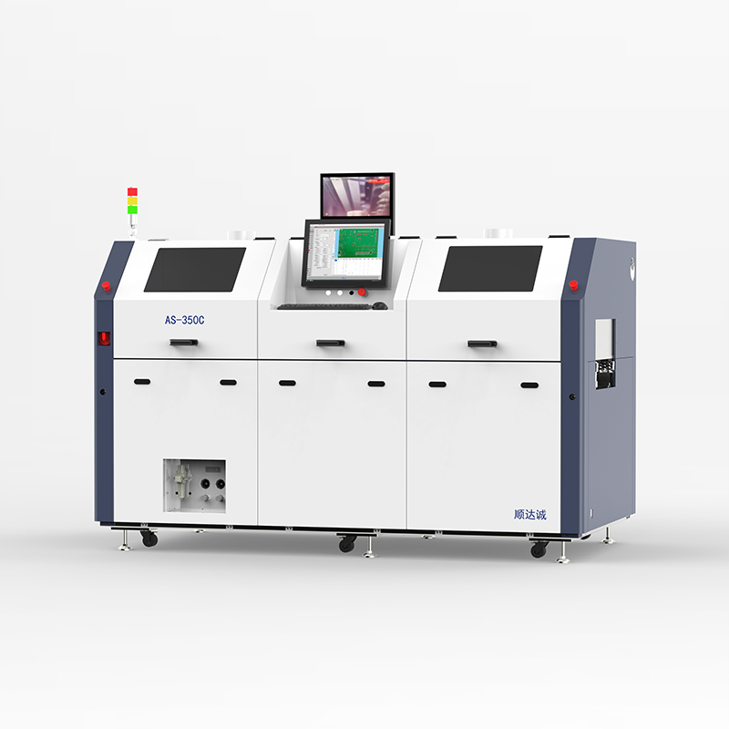
Selective wave soldering is a process that allows for the soldering of specific components on a PCB without affecting the entire board. Unlike traditional wave soldering, which exposes the entire bottom side of the PCB to a wave of molten solder, selective wave soldering targets only designated areas. This precision is achieved through the use of dedicated nozzles that deliver solder to specific points, making it ideal for mixed-technology assemblies where sensitive surface-mount components coexist with through-hole components.
The process involves several critical stages: fluxing, preheating, and soldering. Each stage must be carefully controlled to ensure optimal results. Fluxing cleans the component leads and PCB pads, preheating activates the flux and reduces thermal shock, and soldering forms the mechanical and electrical connections. Any deviations in these stages can lead to defects, underscoring the importance of understanding and optimizing each step.
Common Problems and Their Solutions
Insufficient Solder Wetting
Insufficient solder wetting is a frequent issue in selective wave soldering, characterized by the incomplete coverage of solder on the pad or component lead. This defect can lead to weak mechanical joints and unreliable electrical connections, posing significant risks in applications where reliability is paramount, such as aerospace and medical devices.
The root causes of insufficient wetting often include inadequate preheating, improper flux application, and contamination on soldering surfaces. Ensuring proper preheating is vital; the PCB must reach a temperature that allows the flux to activate fully and the solder to flow properly. A study by the Institute of Printed Circuits (IPC) suggests that the ideal preheating temperature should be approximately 70% of the solder's melting temperature, typically ranging between 100°C and 150°C for most solder alloys.
Flux application is equally critical. Flux removes oxides from the metal surfaces and prevents oxidation during soldering. Utilizing an appropriate flux type and ensuring uniform application are essential steps. Excessive or insufficient flux can both lead to defects. Implementing automated fluxing systems with precise controls can improve consistency. Regular monitoring and maintenance of the fluxing system help in maintaining optimal flux levels.
Contamination on the soldering surfaces, such as oils, dust, or residues from previous processes, can inhibit solder flow. Implementing a robust cleaning protocol before soldering can mitigate this issue. The use of clean room conditions or controlled environments may be necessary for high-precision applications.
Bridging and Solder Shorts
Bridging defects occur when excess solder forms unintended connections between adjacent pads or component leads, resulting in shorts that can compromise circuit functionality. This issue is particularly problematic in high-density PCBs where component leads are closely spaced.
To address bridging, it's essential to optimize solder wave parameters. The solder wave height and angle should be adjusted to ensure that solder contacts the desired areas without overflowing onto adjacent regions. According to research by the Electronics Manufacturing Science Institute, adjusting the conveyor speed and optimizing the PCB's travel angle can significantly reduce bridging occurrences.
Implementing dedicated fixtures or pallets that mask off areas not to be soldered can also be effective. These fixtures can be designed to expose only the necessary parts of the PCB to the solder wave. Moreover, utilizing a customized soldering solution tailored to the specific PCB design can further minimize the risk of bridging.
Component Misalignment
Component misalignment during selective wave soldering can lead to insufficient solder joints, open circuits, or physical damage to components and the PCB. This problem may stem from mechanical vibrations, thermal expansion, or improper handling during the assembly process.
Ensuring that components are securely placed prior to soldering is crucial. This can be achieved by using adhesives or mechanical supports to hold components in place. Additionally, reviewing the design of the soldering fixtures to minimize movement during the process can help. Thermal profiling to understand how the PCB and components expand during heating can inform adjustments to the process parameters, mitigating misalignment due to thermal effects.
Solder Balling
Solder balling refers to the formation of small, spherical solder particles on the PCB surface. These solder balls can cause short circuits and reliability issues, especially in fine-pitch components. Causes of solder balling include excessive flux, rapid heating rates, or contamination on the PCB surface.
To prevent solder balling, controlling the amount and type of flux used is essential. Low-residue or no-clean fluxes can reduce the likelihood of this defect. Adjusting the preheating profile to provide a gradual temperature increase allows for controlled volatilization of flux solvents, reducing spattering. Ensuring that PCBs are clean and free of moisture prior to soldering is also important.
Copper Dissolution
Copper dissolution occurs when the molten solder erodes the copper pads or traces on the PCB. This can weaken the mechanical strength of solder joints and impair the electrical performance of the circuit. High tin-content solders and extended contact times with molten solder exacerbate this problem.
Mitigating copper dissolution involves optimizing the solder alloy composition and minimizing the contact time between the solder and the PCB. Using solder alloys with lower tin content or adding elements like nickel can reduce the rate of copper erosion. Adjusting the conveyor speed to limit the exposure time and employing selective soldering techniques that focus the solder only where necessary can also help.
Optimizing the Selective Wave Soldering Process
Process Control and Monitoring
Implementing rigorous process control measures is essential for minimizing defects in selective wave soldering. This includes regular calibration of equipment, consistent monitoring of process parameters, and thorough documentation. Utilizing statistical process control (SPC) techniques can help identify trends and variances before they lead to defects.
Advanced selective wave soldering machines are equipped with sensors and software that provide real-time feedback on temperature profiles, solder wave characteristics, and flux usage. Operators can use this data to make immediate adjustments, ensuring that the process remains within specified parameters. Regular maintenance schedules for equipment components, such as nozzles and pumps, prevent unexpected downtime and maintain process integrity.
Design for Manufacturability (DFM)
Collaborating with design engineers to optimize PCB layouts for manufacturability can significantly reduce soldering defects. By considering the limitations and capabilities of selective wave soldering during the design phase, issues such as component placement, pad design, and thermal reliefs can be addressed proactively.
Incorporating proper spacing between pads, orienting through-hole components to facilitate solder flow, and providing adequate clearances can enhance soldering outcomes. Additionally, specifying appropriate solder masks and surface finishes can improve wetting and reduce the occurrence of bridging and other defects. Engaging in DFM reviews early in the product development cycle enables the identification and resolution of potential manufacturing issues before they impact production.
Training and Skill Development
The proficiency of operators and technicians plays a crucial role in the success of the selective wave soldering process. Providing comprehensive training on equipment operation, process parameters, and defect identification equips personnel to make informed decisions and adjustments.
Continuing education programs and certifications, such as those offered by IPC or SMTA, ensure that staff remain current with industry best practices and technological advancements. Encouraging a culture of continuous improvement and empowering employees to contribute suggestions can lead to process enhancements and defect reduction.
 Advanced Technologies and Innovations
Automation and Industry 4.0 Integration
The integration of automation and Industry 4.0 principles into selective wave soldering offers significant potential for improving process efficiency and quality. Automated systems can handle complex tasks with high precision and repeatability, reducing human error and variability.
Implementing advanced robotics for PCB handling, flux application, and inspection enhances consistency. Machine learning algorithms can analyze vast amounts of process data to predict defects and suggest optimal settings. Connectivity between machines and centralized monitoring systems facilitates real-time decision-making and fosters a more agile manufacturing environment.
Lead-Free Soldering and Environmental Considerations
The global shift towards lead-free soldering, driven by environmental regulations such as the Restriction of Hazardous Substances Directive (RoHS), presents new challenges and opportunities. Lead-free solders typically have higher melting temperatures and different fluid dynamics, requiring adjustments to the soldering process.
Manufacturers must optimize their selective wave soldering machines to accommodate these changes, including adjusting preheating temperatures, conveyor speeds, and solder wave parameters. Research indicates that using alloys like SAC305 (tin-silver-copper) can provide comparable performance to traditional lead-based solders when properly implemented.
Additionally, adopting environmentally friendly fluxes and implementing waste management protocols aligns with corporate sustainability goals and regulatory requirements. These practices not only reduce environmental impact but can also enhance the company's reputation and competitiveness in the market.
Conclusion
Selective wave soldering machines are powerful tools in the electronics manufacturing industry, enabling the production of sophisticated PCBs with precision and efficiency. However, the complexity of the process introduces several challenges that can impact product quality and production throughput. By understanding the common problems such as insufficient solder wetting, bridging, component misalignment, solder balling, and copper dissolution, manufacturers can implement targeted strategies to mitigate these issues.
Optimizing process parameters, investing in advanced technologies, and fostering a skilled workforce are key factors in enhancing the selective wave soldering process. Moreover, collaborating on design for manufacturability and embracing innovations like automation and lead-free soldering contribute to continuous improvement and sustainable practices.
For manufacturers seeking to improve their soldering processes, leveraging expertise and customized soldering solutions can provide a competitive advantage. By addressing the challenges proactively and embracing advancements, companies can achieve higher quality, greater efficiency, and better alignment with industry trends.
Dongguan Sundarc Automation Technology Co., Ltd. (Shenzhen Sundarc Electronic Equipment Co., Ltd.) was founded in 2010, is a collection of research and development, production and sales as one of the "national high-tech enterprises". Mainly committed to research and development of high-grade selective wave soldering equipment.Quick Links
Contact Us
+86-18029195527 +8618029190631 Located in 4th Floor, Block B, Building 5, Guanghui Wisdom Valley, No,136, Yongjun Road, Dalingshan Town, Dongguan city, Guangdong province.Copyright © 2025 Dongguan Sundarc Automation Technology Co., Ltd. All Rights Reserved. Sitemap


